Electronic High/Low Game Mar. 26, 2014 in 6thform, Assembly, Electronics, Games, Text
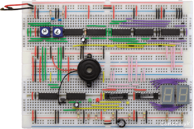
To start the game, the player will press either button which draws the starting card; once drawn, the player will need to choose if they think the next card will be higher or lower than the current card and press the corresponding button. If they are right the green LED will light up, if not the red LED will light up and the buzzer will sound.
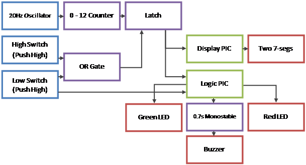
Explanation + Specification
| 20Hz Oscillator | A relaxation oscillator that produces a 20Hz square wave which oscillates between 0V and +5V. It clocks the counter. | |
| 0 - 12 Counter | A binary counter that resets when 13 is output using two AND gates. I am using 4 outputs. | |
| Latch | A 4 bit latch which copies what is at the input to the output when clocked by the OR gate. | |
| Switches | Two switches which are used to guess. Outputs 0V when released, +5V when pressed. | |
| OR Gate | An OR gate that ORs together both of the switches before sending the signal to the clock input of the latch. This then will select a new card. | |
| Display PIC and 7 segment | Takes the 4 bit word from the latch and displays a card (A, 2, 3, 4, 5, 6, 7, 8, 9, 10, J, q or K) on the two seven segment displays. | |
| Logic PIC and two LEDs | Determines if the user has guessed correctly. If the player is correct, it lights the green LED and turns off the red LED; if not, it turns on the red LED, sends a 5ms pulse to the monostable and turns off the green LED. | |
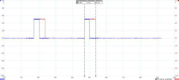
| Monostable and Buzzer | Produces a 0.7s pulse which powers a MOSFET which causes the buzzer to sound. Runs asynchronously to the rest of the circuit. |
Testing
I plan to use Picoscope (A multi-input computer oscilloscope) along with photos to provide evidence of a functioning circuit; to help me build I may use a logic probe and voltmeter.
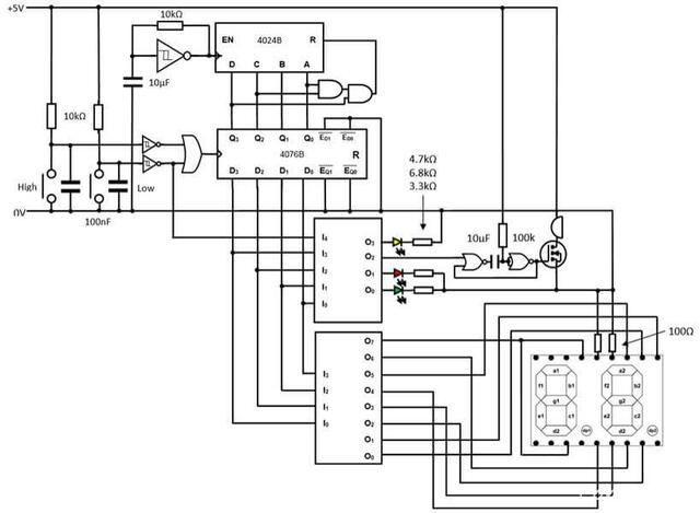
Circuit Diagram
Sub-Systems
Clock Sub-System
Summary and Specification
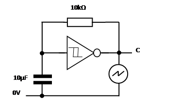
This counter will constantly create pulses which will be sent to the 0 - 12 counter so that, by using the randomness of the player’s timing, we can generate pseudo-random numbers so that the player has to guess. This will be achieved using a relaxation oscillator constructed from an inverting Schmitt trigger along with a resistor and capacitor.
I plan to use a 10kΩ resistor and a 10μF capacitor to achieve a frequency of 20Hz.
 |  |
 |  |
 |  |
This is a circuit from OCR Electronics for AS by Michael Brimicombe.
Diagrams
Testing Plan
I will connect up Picoscope to the clocks output and measure 10 pulses and then divide by 10 to get the period of a single pulse. Now, using:
I will calculate the frequency and see if it matches my predicted frequency. If it does, great; if not, it doesn’t matter that much due to how I am using it to generate pseudo-random numbers, a task that does not need a super precise clock.
Evidence
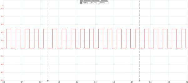
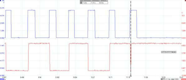
Connection: Clock Output
| T1 / ms | T2 / ms | 10T / ms | T / ms | F / Hz |
|---|---|---|---|---|
| 240.6 | 741.7 | 501.1 | 50.11 | 19.96 |
Analysis
I predicted a frequency of 20Hz and got 19.96Hz, a 0.2% difference; this is extremely close to my calculated frequency. This worked correctly when it was first powered; I did not require any help to get this working correctly.
Sources
- OCR Electronics for AS by Michael Brimicombe page 43
- OCR Electronics for AS by Michael Brimicombe page 159
0 - 12 Counter Sub-System
Summary and Specifications
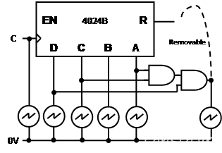
This counter will receive pulses from the Clock and increment until it reaches 13 in which case it will nearly instantly reset to 0. This will be achieved with AND gates between O~0~, O~3~ and O~4~ connected to the counters reset pin. This counter, along with the clock will be what creates the pseudo-random numbers used in my circuit - I plan to use a 4024B chip.
This circuit is based on one by Michael Brimicombe in OCR Electronics for AS.
Diagram
Testing Plan
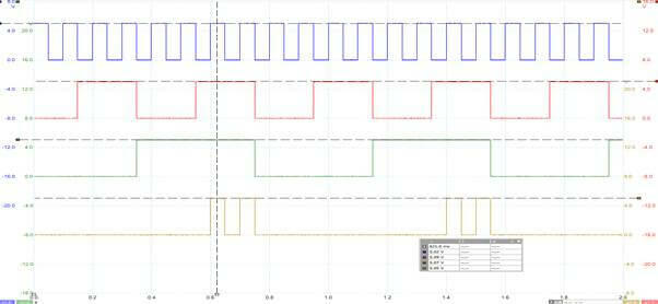
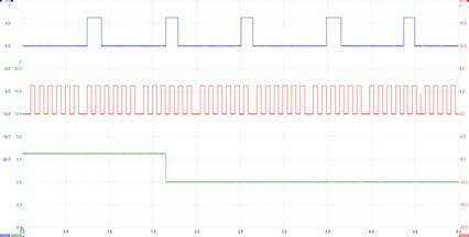
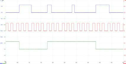
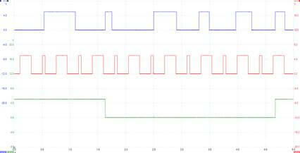
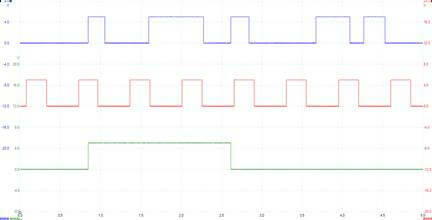
- Connect up my working clock to the clock input and record the output of clock, A, B and C without the AND gates added using Picoscope.
- Remove clock and connect up D to Picoscope.
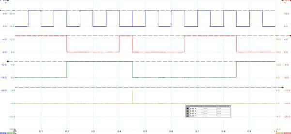
- Add the AND gates to connect to A, C and D to see when they would trigger a reset (The output of the second AND gate will not currently be connected to the reset pin). Measure A, C, D and reset with Picoscope.
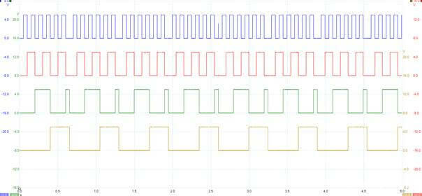
- Connect the output of the AND gates to the reset pin and test the entire sub-system fully assembled and record both A, C, D and clock as well as A, B, C, D.
Evidence
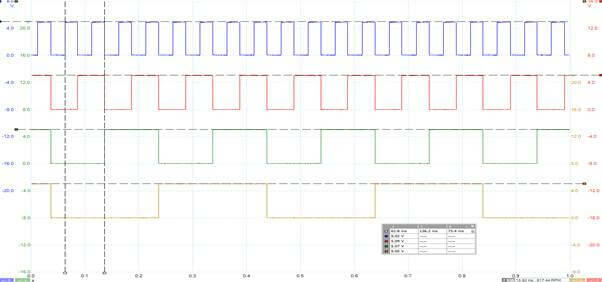
Connections: Clock, A, B, C. Reset is not connected.
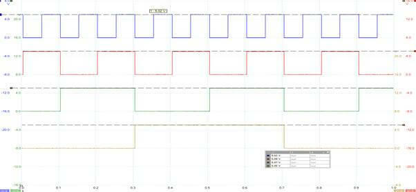
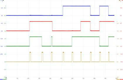
Connections: A, B, C, D. Reset is not connected.
Connections: A, C, D, Reset. Reset is not connected.
Connections: A, C, D, Reset. Reset is connected.
Connections: A, B, C, D. Reset is connected.
Pulse Table
| Pulse | State | Pulse | State | Pulse | State | Pulse | State | |||
|---|---|---|---|---|---|---|---|---|---|---|
| 0 | 0000 | 4 | 0100 | 8 | 1000 | 12 | 1100 | |||
| 1 | 0001 | 5 | 0101 | 9 | 1001 | 13 | 0000 | |||
| 2 | 0010 | 6 | 0110 | 10 | 1010 | 14 | 0001 | |||
| 3 | 0011 | 7 | 0111 | 11 | 1011 | Now it loops |
Analysis
As you can see, the counter works correctly and you can clearly see it count from 0 to 12; on some of the traces you can even see the 13 ^th^ pulse. It worked first time without needing troubleshooting.
Sources
- OCR Electronics for AS by Michael Brimicombe page 8
- OCR Electronics for AS by Michael Brimicombe page 10
Latch Sub-System
Summary and Specifications
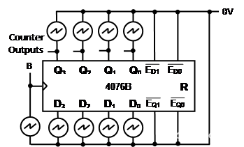
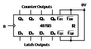
When the OR gates output goes high due to player input; the latch will copy the output nibble from the latches input to the latches output. This output will be connected to the inputs of both of the PICs. I will use a 4076B chip.
Diagrams
Testing Plan
I will connect up Picoscope to the clock input, one input and its corresponding output and test if whatever I put at the input gets copied to the output. If it does for each latch, then the sub-system is fully functional.
Evidence
Player Input Input A. Output A.
Player Input Input B. Output B.
Player Input Input C. Output C.
Player Input Input D. Output D.
Debugging issues
Connections: O~A~, O~B~, O~C~, Player Input
The problem - triggering twice meant the display flickered and the Logic PIC ran twice. Fixed with a Schmitt and capacitor on the switches.
The noise at the end caused the double trigger.
Connections: Player Input, Success from Logic PIC
Analysis
While in most cases the latch worked, further down the line I discovered it occasionally triggered twice. To remedy this, my teacher suggested using a capacitor and an inverting Schmitt trigger to remove noise from the push buttons, which was the cause of the double triggering.
Another hard to diagnose issue was that rarely; the short 13^th^ pulse was picked up and copied to the latch output. I had made my PICs to trust any input, valid or invalid, causing an issue. My solution was to check the value in the PIC and if it was invalid, do nothing. If I decided to make it take an action, I would end bias the pseudo-random numbers in favour of 12.
After this change, it worked correctly all of the time.
Sources
- OCR Electronics for AS by Michael Brimicombe page 159
Switches (Player Input) Subsystem
Summary and Specifications
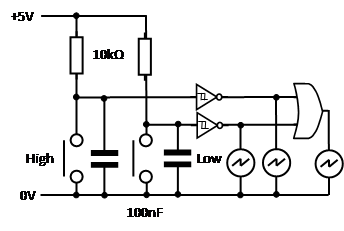
I have two push switches which will output 0V when released and +5V when pressed by the player. I will connect them up to an OR gate and use that as the clock pulse for the latch and I have connected the low switch to the Logic PIC so that it can determine which button the player pressed.
Due to previously mentioned noise, I added a capacitor and non-inverting Schmitt trigger on the output of the switches, so that any component only triggers once. The capacitance of the capacitors is 100nF, enough to smooth the noise but not slow the switches. The time constant is 1ms.
The original design was inspired by one in OCR Electronics for AS.
Diagram
Original
Testing Plan
To test I will connect up the output of the two switches and the OR gate to Picoscope, one at a time, to test that the OR gate and the switches work.
Evidence
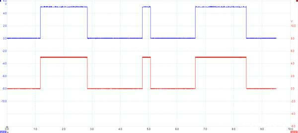
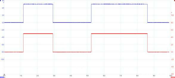
Connections: High Switch, OR Output.
Connections: Low Switch, OR Output.
Analysis
The switches appeared to work perfectly first time, however when I connected the OR to the latch I noticed that the latch occasionally triggered twice; this was due to noise created when releasing the switch. After putting in the capacitor and inverting Schmitt trigger on my teacher’s advice, the problem was fixed.
Sources
- OCR Electronics for AS by Michael Brimicombe page 159
- OCR Electronics For As by Michael Brimicombe Page 1
Display PIC Sub-System
Summary and Specifications
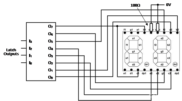
Will take a nibble (4 bit number) as an input and by using a lookup table with the nibble as the pointer, display a card using both of the 7-segment displays. The first display will show 1 or nothing with one of the output pins connected too it. The second display will show A, 2, 3, 4, 5, 6, 7, 8, 9, 0, J, q or K.
For the 7-segment displays I am using, it is suggested to have 5mA per segment.
As I ended up using the 18-pin PICAXE chip I could not use the language I was taught for A2. I wanted to use a lookup table so I ended up researching, and then eventually using PICAXE BASIC over the flowcharts.
Diagram
Testing Plan
I will input a number 0 - 12 to the PIC input and take a photo of the result. If I get A, 2, 3, 4, 5, 6, 7, 8, 9, 10, J, q, K out it works. Due to the programming, entering anything higher will not solicit a response.
Output Bytes
After finishing wiring up the 7 segment display, I created this table for each character I wanted to display; so that I knew which values I need to use in the lookup table.
| Display | Segments | Binary | Reversed | Hexadecimal | Binary |
|---|---|---|---|---|---|
| A | abcefg | 0101 1111 | 1111 1010 | FA | 250 |
| 2 | abdeg | 0011 1011 | 1101 1100 | DC | 220 |
| 3 | abcdg | 0110 1011 | 1101 0110 | D6 | 214 |
| 4 | bcfg | 0100 1101 | 1011 0010 | B2 | 178 |
| 5 | acdfg | 0110 1110 | 0111 0110 | 76 | 118 |
| 6 | acdefg | 0111 1110 | 0111 1110 | 7E | 126 |
| 7 | abcf | 0100 0111 | 1110 0010 | E2 | 226 |
| 8 | abcdefg | 0111 1111 | 1111 1110 | FE | 254 |
| 9 | abcdfg | 0110 1111 | 1111 0110 | F6 | 246 |
| 10 | bc abcdef | 1111 0111 | 1110 1111 | EF | 239 |
| J | abcd | 0110 0011 | 1100 0110 | C6 | 198 |
| q | abcfg | 0100 1111 | 1111 0010 | F2 | 242 |
| K | bcefg | 0101 1101 | 1011 1010 | BA | 186 |
| - | g | 0000 1000 | 0001 0000 | 10 | 16 |
Program
init:
	' We don't want to always display A at the start
	let pins = $10
	if pins != 0 then
	goto display
	endif
	goto init
.
display:
	' Temporary variable
	let b0 = pins
.
	' Create a nibble of i1,i0,i7,i6 (18X has a weird layout)
	let b1 = b0&2/2
	let b2 = b0&1*2
	let b3 = b0&128/32
	let b4 = b0&64/8
.
	' PICAXE's language doesn't support BIDMAS or even brackets!
	let b5 = b1 + b2 + b3 + b4
.
	' Check in input nibble is valid
	if b5 < 13 then
	' Retrieve char from LUT (Displays A,2,3,4,5,6,7,8,9,10,J,q,K) and display
	lookup b5,($FA,$DC,$D6,$B2,$76,$7E,$E2,$FE,$F6,$EF,$C6,$F2,$BA),pins
	endif
.
	goto display
Evidence
| Input | Photo | Input | Photo | Input | Photo |
|---|---|---|---|---|---|
| 0000 | 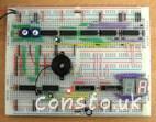 | 0001 | 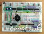 | 0010 | 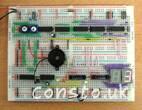 |
| 0011 | 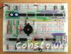 | 0100 | 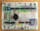 | 0101 | 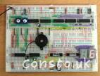 |
| 0110 | 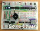 | 0111 | 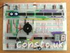 | 1000 | 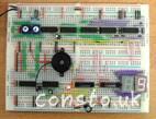 |
| 1001 | 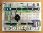 | 1010 | 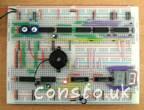 | 1011 | 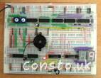 |
| 1100 | 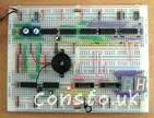 | Initial State | 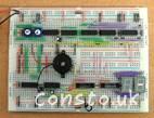 |
Analysis
As I created the values for the lookup table after wiring up the 7 segment display I didn’t encounter many issues associated with only the PIC and 7 segment display. The only problem encountered was solved by reversing the byte. I didn’t require assistance for this.
I did however encounter a problem with it ‘flashing’, this was due to the latch triggering twice; I fixed this by adding a capacitor and inverting Schmitt to my switches.
Sources
- OCR Electronics for AS by Michael Brimicombe page 159
- http://www.picaxe.com/BASIC-Commands
- http://www.picaxe.com/docs/picaxe_manual1.pdf
Logic PIC and LEDs Sub-System
Summary and Specifications
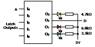
After the player has pressed a button once, the Logic PIC will have a number 0 - 12 stored. When the number changes, it will compare the new number to the stored number. If the player made the correct guess the green LED will light up and the red LED will turn off. If the player was incorrect, the green LED will turn off, the red LED will turn on and the monostable, connected to the buzzer, will sound for a fixed time. This will repeat indefinitely while the circuit is powered.
The yellow LED will toggle each time the user guesses. This was added for debug purposes.
Assuming 1mA. When testing, the red and the yellow LED were too bright so I opted for larger resistors: 6.8kΩ and 4.7kΩ for them.
Diagram
Testing Plan
I will test this by testing it out in the context of the completed circuit.
Program
init:
	let pins = 0

	' Temporary variable
	let b0 = pins
	' Create a nibble of i1,i0,i7,i6 (18X has a weird layout)
	let b1 = b0&2/2
	let b2 = b0&1*2
	let b3 = b0&128/32
	let b4 = b0&64/8
	' PICAXE's language doesn't support BIDMAS or even brackets!
	let b7 = b1 + b2 + b3 + b4
.
	if b7 = 0 then
	goto init
	endif

	' Stores the state of the yellow LED
	let b10 = 1
.
logic:
	' Same as above
	let b0 = pins
	let b1 = b0&2/2
	let b2 = b0&1*2
	let b3 = b0&128/32
	let b4 = b0&64/8
	let b6 = b1 + b2 + b3 + b4
.
	' If a new, valid number appears we continue, else loop
	if b6 = b7 or b6 > 12 then
	goto logic
	endif
.
	' b5 = Low button pressed
	let b5 = b0&4/4
	' If new number greater than old
	if b6 > b7 then
	' 1 = correct, 6->2 incorrect
	lookup b5,(1,6),pins
	pause 5
	lookup b5,(1,2),pins
	else
	lookup b5,(6,1),pins
	pause 5
	lookup b5,(2,1),pins
	endif
.
	' Copy the current number to old number
	let b7 = b6

	' Toggles the yellow LED
	if b10 = 1 then
	high 3
	b10 = 0
	else
	low 3
	b10 = 1
	endif
.
	goto logic
Evidence
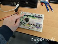
Me guessing correctly.
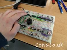
Guessing incorrectly, the buzzer sounded.
Once the previously mentioned bugs were squashed; when I tested out the entire circuit it worked.
Analysis
After a bumpy start related to two undiscovered problems (Latch double triggering and 13 occasionally being selected) it worked correctly.
Sources
- OCR Electronics for AS by Michael Brimicombe page 159
- http://www.picaxe.com/BASIC-Commands
- http://www.picaxe.com/docs/picaxe_manual1.pdf
- OCR Electronics For As by Michael Brimicombe Page 7
Monostable and Buzzer Sub-System
Summary and Specifications
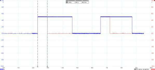
The monostable will get a short high pulse from the Logic PIC and trigger the buzzer for 0.7 seconds. This will allow the Logic PIC to continue functioning without being concerned if the buzzer still needs to be powered. I will be using a 100kΩ resistor with a 10μF capacitor.
This design is based on the NAND gate monostable in OCR Electronics for AS; they are very similar however the NAND gate monostable produces a low pulse as opposed to a high pulse.
Diagrams
Testing Plan
I will connect up Picoscope to the input and output of the monostable to test the length of the pulse produced; I will listen to the buzzer to see if it sounds in the completed circuit.
Evidence
Connections: Input, Output Pulse
Connections: Input, Output Pulse
| T1 / s | T2 / s | ΔT / ms | T1 / s | T2 / s | ΔT / ms |
|---|---|---|---|---|---|
| 2.298 | 2.961 | 663 | 5.367 | 4.712 | 655 |
Analysis
For both short and long input pulses, the monostable produced reliable length pulses of around 659ms; this is 5.86% off my calculated value of 700ms. This is accurate enough for my use as I all I need from this is a short pulse that can be easily created using a monostable. If I needed it to be more accurate I would use a variable resistor.
Originally the MOSFET did not work correctly; I ended up concluding it was a dead MOSFET. This fixed this sub-system.
Sources
- OCR Electronics For As by Michael Brimicombe Page 41
- OCR Electronics For As by Michael Brimicombe Page 11
- OCR Electronics for AS by Michael Brimicombe page 159
Conclusion
Despite a few setbacks along the way due to unforeseen problems, I produced a good High/Low game that is fun to play. It may have a few, minor flaws (including the fact Ace cannot be the first card drawn) but I feel I have achieved what I set out to do. Overall I am happy with what I have designed, created and finally tested.
I believe that my circuit meet my specification.
During the later stages of testing, me and the other pupils in my class experimented with each other’s projects. In their final testing, my high/low game worked correctly and they enjoyed making a guess.
